


Material[]
This material is usable for publication or reproduction, provided the following source information is visibly included at all times: "FACETS Project, www.facets-project.org". Please use the provided image-captions or an adequate translation to document the contents of the respective image.
| FACETS - An Introductory Presentation | pdf-file (1.1 MB) |
| Karlheinz Meier, Electronic Vision(s) Group, Heidelberg A set of presentation slides that provide an introductory overview on the FACETS project, its motivation, goals, and structural organization | |
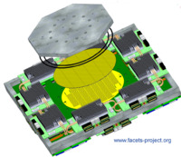
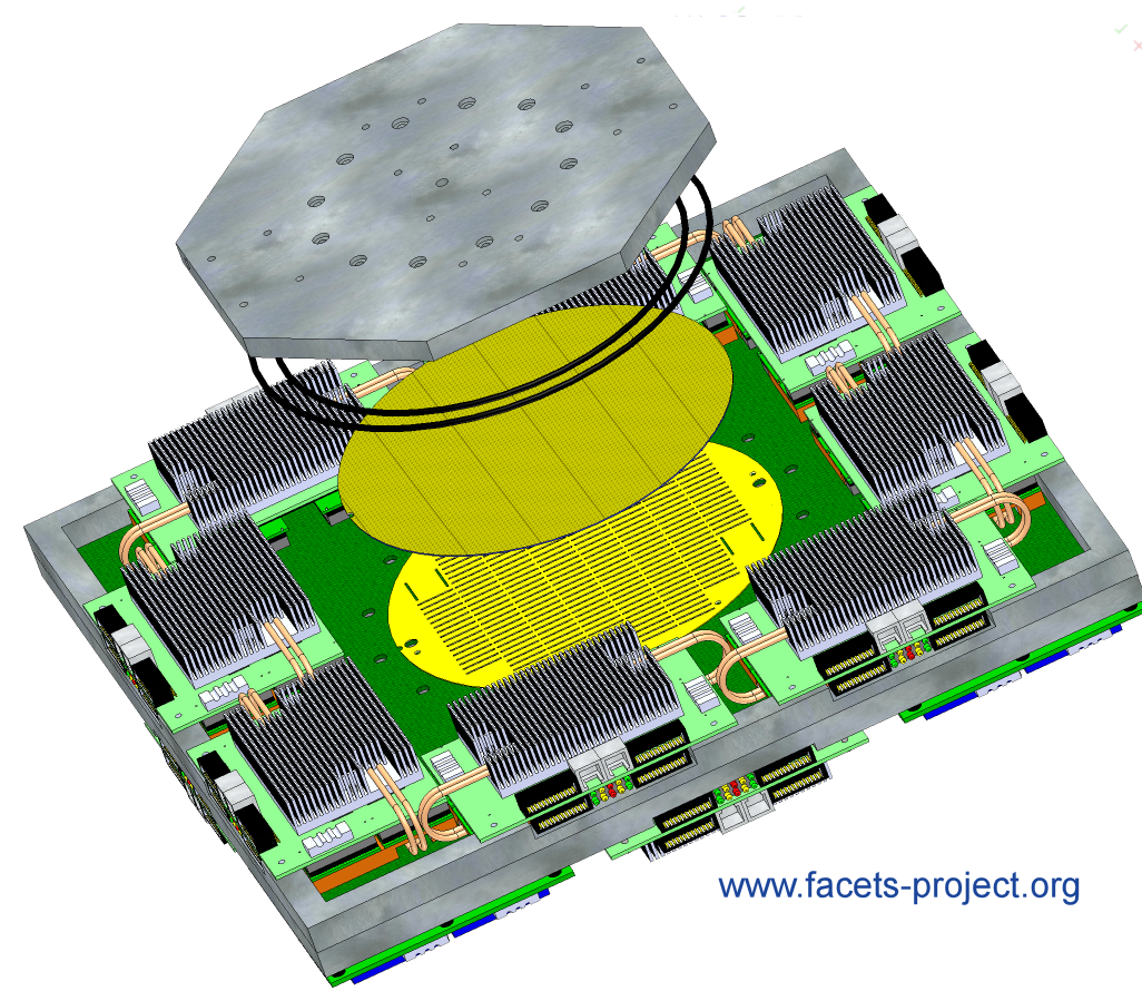
| Design Study of a Neural Network Hardware Using Wafer Scale Integration | jpg-file (250 KB) |
| Jonathan Meier, Heidelberg Recommended caption text: Design Study of a Neural Network Hardware Using Wafer Scale Integration | |
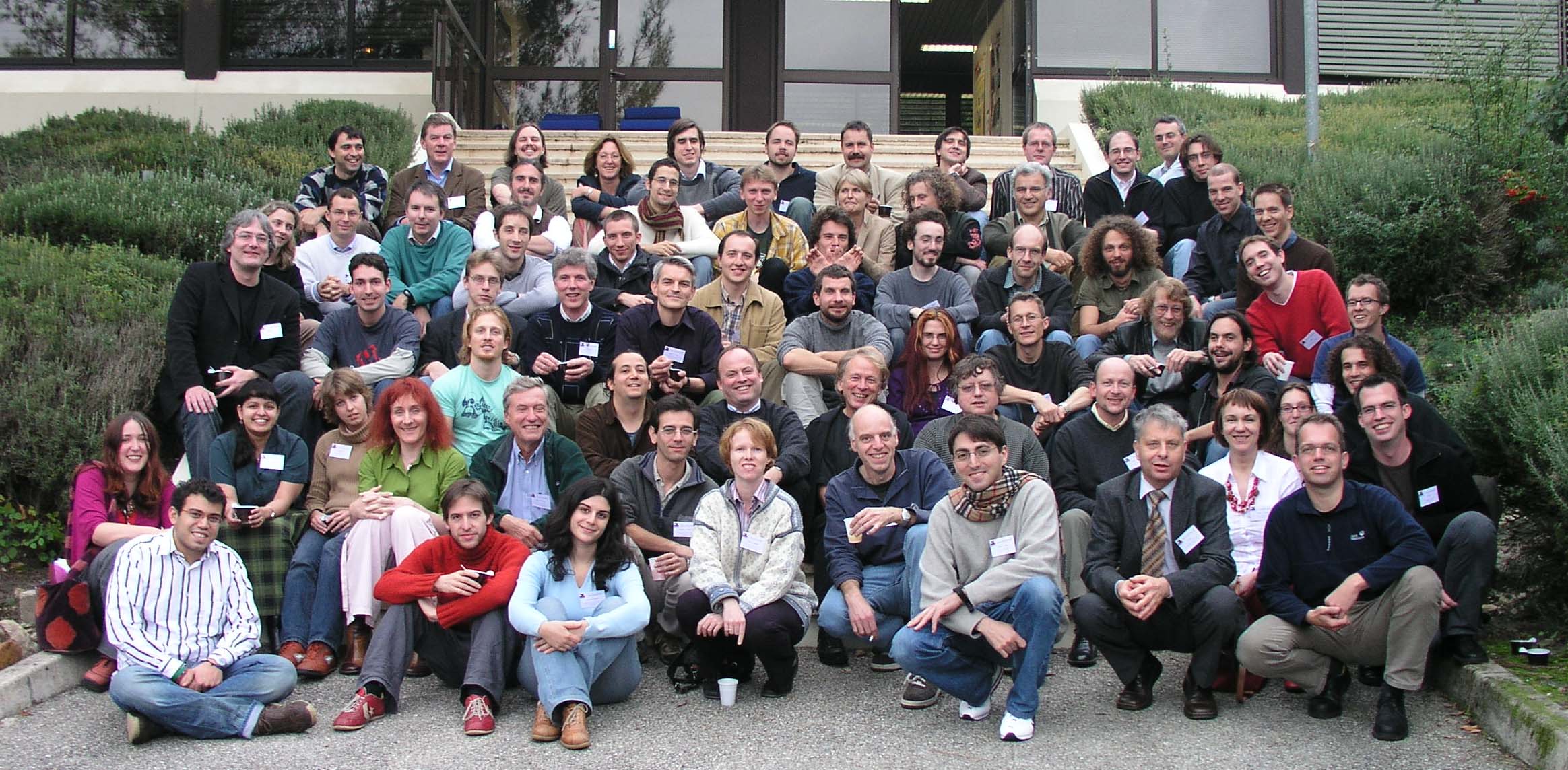
| Photograph of the members of the FACETS project | jpg-file (390 KB) |
| Photograph taken by Marie-Cecile Lafont during the FACETS Kickoff Meeting, November 3rd-5th, 2005 at INRIA, Sophia-Antipolis, France Recommended caption text: Members of the FACETS project at the FACETS Kickoff Meeting, November 2005 |
Presentations[]
- The hardware of the FACETS project in a presentation VLSI Implementations of Very Large Scale Neuromorphic Circuits given on ESSCIRC/BIECS 09 by Johannes Schemmel from 2009 (8MB .pdf)
Image set[]
Please cite the "FACETS project (www.facets-project.org)" when using these images:
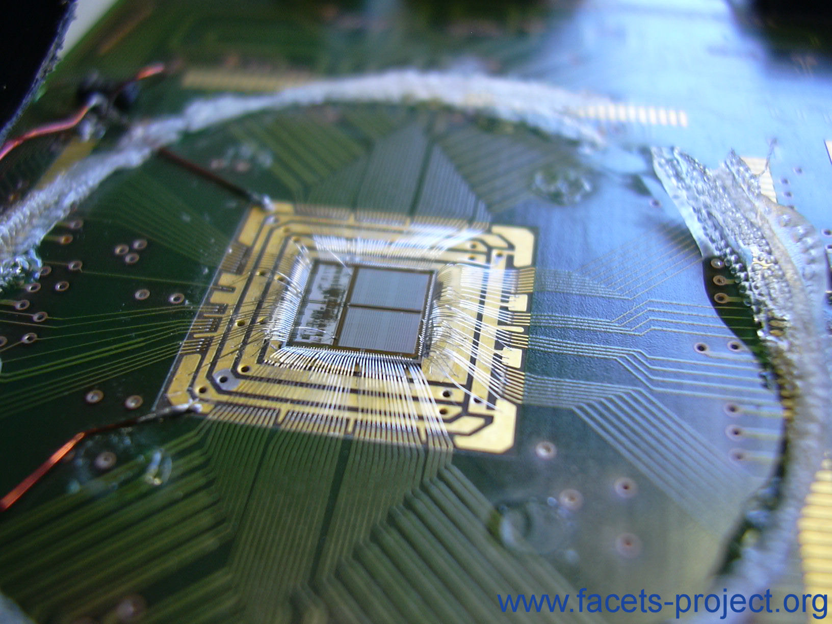
Stage I (Spikey)[]
 | 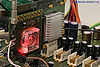 | 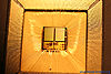 |  |  |
| Membrane voltage trace large image (0.7 MB) | Spikey board on backplane large image(1.1 MB) | Spikey chip large image (1.6 MB) | Spikey chip large image (0.3 MB) | Spikey chip large image (0.7 MB) |
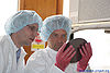
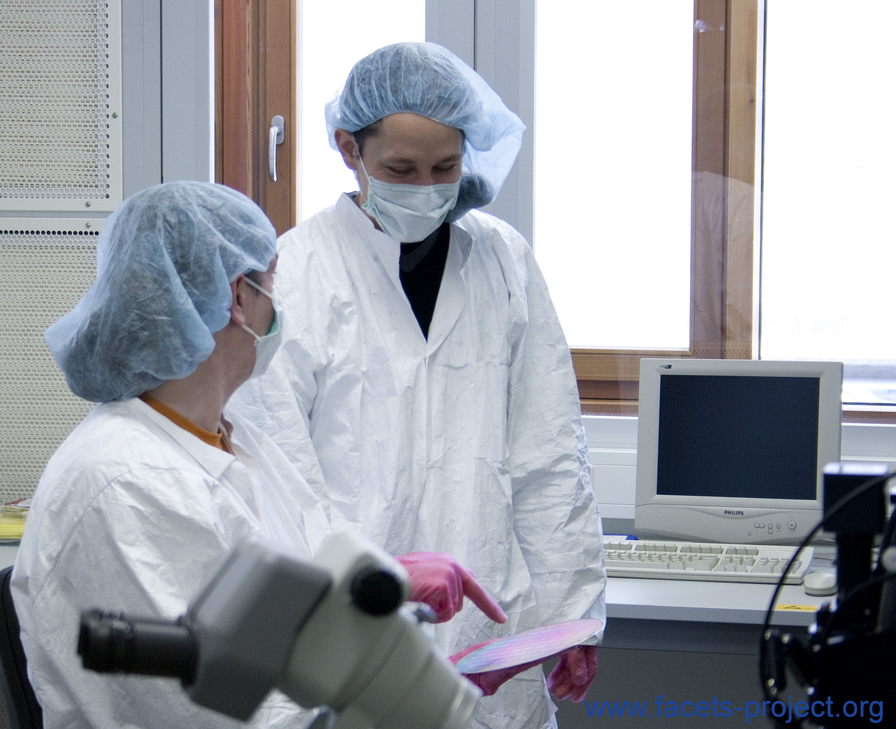
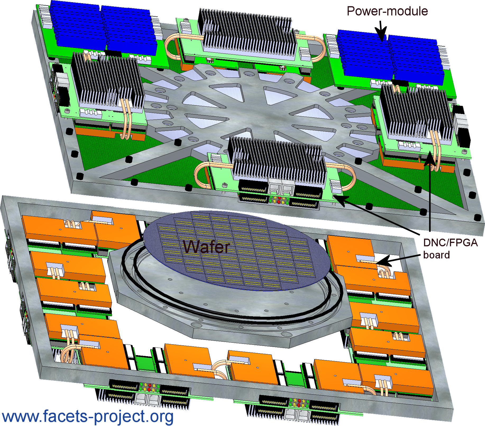
Wafer-handling[]
The Stage II system will use a complete post-processed wafer (instead of single chips) with interconnected electronic representations of neurons and synapses.
 |  |  |
| large image (0.9 MB) | large image (0.6 MB) | large image (0.8 MB) |
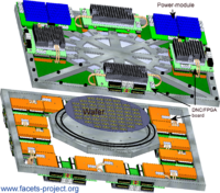
Stage II (wafer-scale system)[]
 |  |
| description and larger image | description and larger image |